Basics of Photovoltaics
Photovoltaic Materials : There are number of materials showing photovoltaic properties. The commonly used materials are Silicon (Si), Cadmium (Cd). Gallium Arsenide (GaAs). These have comparatively better performance over the other materials having solar photovoltaic properties. The materials have to be fabricated in the form of arrays. The process of fabrication is very costly.
Basic Principle of Operation :
All materials may be classified into the following categories :
- Conductors
- Insulators
- Semiconductors
Their salient characteristics are described below :
Conductors :
They have large number of free electrons which are free to move. Hence when a potential is applied, these electrons move at a velocity towards the positive electrode leading to the generation of an e.m.f.
Insulators :
These materials do not have any free electrons and hence they never conduct electricity.
Semiconductors :
These are in between a conductor and insulator. They have few electrons in the orbit which enables them to partially conduct electricity. When a semiconductor is in a crystalline form, they are arranged in a orderly array. They have either four or five electrons only. But when certain impurities are introduced, their conductivity increases considerably. This is shown in Figure A.
 |
| Figure A |
As could be seen each silicon atom is surrounded by four other Silicon atoms having four electrons each. They share four electrons with each of these neighbouring electrons forming a covalent bond. Thus there is no free electron.
N Doped Semiconductor (Donor Impurity) :
When Si is doped by Phosphorous (P) they cannot form a lattice by sharing all the electrons, because Phosphorous has five electrons but Silicon has only four . Hence one of the atoms of P will not be able to share and this will remain as free electron. This free electron is shown in Figure B.
 |
| Figure B |
P Doped Semiconductor (Acceptor Impurity) :
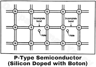
In this case silicon is doped with Boron. Boron has only three electrons in the valance shell. Thus out of the four electrons of Silicon only three will be able to form a covalent bond with the Boron. There will be a deficiency of one electron there by creating a net positive charge. This positive charge is called a ‘hole’. The impurity in this case is called an acceptor impurity. When a semiconductor is so doped with a acceptor impurity it is called a P-type semiconductor. This is shown in Figure C.
 |
| Figure C |
P-N Junction :
When a P-type and N-type semiconductors are joined together we get a P-N junction at the boundary of the two junctions . This is because the electrons in the N-type semiconductor will get attracted by the positive charge of the P-type semiconductor and they will move across the junction . Similarly the holes in the P-type semiconductor will diffuse to the N-type semiconductor. Once the diffusion is complete, there shall be no further diffusion. After this, at P-N junction a permanent electric field will be established. P-N junctions are formed by processes called implanting, diffusion or growing N-type impurity in P-type semiconductor or P-type impurity in N-type semiconductor.
 |
| Figure D |
When a P-N junction receives energy in the form of light or heats the potential gradient increases and leads to a current flow. When the current flow is caused due to the incidence of light, it is called a photovoltaic current.
