McMurray Commutation
Q. Sketch circuit diagram of McMurry Bedford Inverter. How commutation of SCR is done ?
Q. Which type of commutation is used in the Mcmurray Bedford inverter?
Q. What is Mcmurray inverter?
Q. McMurray commutation circuit
Q. MC Murray Inverter
Q. Mcmurray bedford inverter
Circuit Diagram of McMurray Commutation
The circuit configuration for the McMurry half bridge inverter is as shown in Figure A.
S1 and S2 are the main thyristors D1 and D2 are the main diodes, where as S1A S2A D1 and D2 are all auxiliary thyristors and diodes respectively. S1A, S2A, D1A, D2A along with L and C form the commutation circuit for the main thyristors.
 |
| Figure A |
Operation of McMurray Commutation
The operation with an inductive load is explained with the following assumptions :
- The load inductance is large enough, so that the current during commutation interval is constant.
- All the devices work as ideal switches.
- L and C ideal elements having no resistance.
The operation of the circuit can be divided into five modes of operation.
SCR1 is already in conduction, supplying current to the inductive load.
- All the other devices (thyristors or diodes) are in the off state. The commutation capacitor C has been charged to supply voltage V with a polarity as shown in Figure B.
Mode I (t = 0 to t = t1) :
- When S1 is to be commutated, at t = 0 the auxiliary SCR, S1A is turned on. The value of load current at this instant is L1 and as per our assumption it will remain constant during the commutation interval of S1.
- The capacitor discharge current IC flows through the loop L, S1, S1Aand C as shown in Figure C.
- Note that we direction of IC through exactly opposite to that of Io.
- Therefore the net current through SCR1 discharge current exactly equal to the load current starts increang because IS1 = IO – IC. At t = t1 , the discharge current is exactly equal to the load current IO = (IC = IO) hence IS1 = 0 and SCR1 commutated.
 |
||
Figure B
|
Mode II (t1 to t2) :
- The capacitor current further increases, (see Figure D) with beyond the level of output current IO.The excess current (IC – IO) starts flowing through D1.
- The capacitor discharge current increases sinusoidally upto Im and then decreases. At t = t2 capacitor current is again equal to IO (IC – IO) and the current through D1 reduces to zero as ID = IC – IO
- During the period (t2 – t1) = tC diode D1 conducts applying a negative voltage of one diode drop across S1. The equivalent circuit for mode II is as shown in Figure D. Also note that the capacitor charges in the opposite direction.
Mode III (t2 to t3) :
- At t = t2 the capacitor current is equal to IO and reduces further. Therefore after t = t2 the capacitor current cannot maintain the load current.
- The inductive load therefore induces a self induced voltage to forward bias diode D2. Thus diode D2 supplies the remaining load current as IO = IC + ID2
where IC is less than IO’
IL
ID2
- The current path for log is as shown in Figure E. This current flows through D2 due to the stored energy in the inductive load.
- Thus the stored energy in the load is fed back to the lower half of the power supply. At t = t3 the capacitor current IC = 0 and the auxiliary thyristor S1A is turned OFF.
- The voltage on the commutating capacitor is greater than V due to the presence of L in series with it. This completes the commutation action of S1.
 |
| Figure D |
 |
| Figure E |
Mode IV (t3 ≤
t ≤ t4) :
- At t = t3 entire load current is transferred to D2 so it will be decreasing as shown in the Figure I. For mode IV this current flows through D2, load, V / 2 back to D2.
- The voltage on the capacitor C is greater than the supply voltage V therefore the capacitor discharges through D1A (the auxiliary diode), supply V, D2 L and C as shown in the Figure F.
- The capacitor current ICis therefore negative for this mode of operation. At t = t4, IC = 0
Mode V (t4 ≤
t ≤ t5) :
- The only current that flows in the circuit is ID2 and IO = ID2. This current is due to the stored energy in the inductive load,
- The load current continues to decrease and finally at t5 goes to zero. Diode D2 is turned off and thyristor S2 can be turned on (See Figure G).
 |
| Figure F |
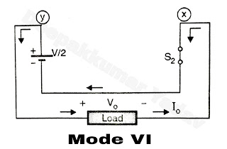
Mode VI (t4 ≤ t ≤ t5) :
- At t = t5, the load current flowing through the diode D2 reduces to zero, and the thyristor S2 can be turned on.
- The load voltage and current both will be negative as shown in Figure H.
- SCR2 can be turned off by turning on the auxiliary SCR, i.e. SCR2 A.
- The McMurry commutation is thus a forced commutation in which a current in opposite direction is forced to turn off a conducting SCR. This is therefore a forced current commutation.
- The same McMurry commutation can be used for the single phase bridge inverter as shown in Figure
 |
| Figure H |
 |
| Figure I |
 |
| Figure J |


