Parallel Inverter or Centre Tapped Inverter (with Inductive Load)
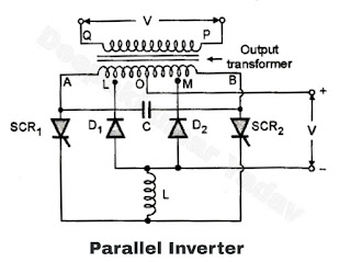
- Figure A shows the schematic diagram of a 1Φ parallel inverter. SCRs 1 and 2 are the main load carrying SCRs.
- L and C are the commutating components. Diodes D1 and D2 permit the load reactive power to be fed back to the supply and feed back the stored energy on the commutation components to the load. These are called as the feedback diodes.
Operation Parallel Inverter or Centre Tapped Inverter :
Mode I (t0 – t1) :
- In mode I the load voltage is positive and load current is negative. Hence the stored energy is returned back from load to source, via the feedback diodes.
- This mode is similar to mode IV.
Mode II (t1 – t2) :
- At instant t1, the SCR2is turned on. Neglecting the small drop across the inductance, the supply voltage V appears across the left half of primary winding OA.
- By transformer action, terminal B will be at a potential of 2 V Volts with respect to terminal A.
- Thus the capacitor charges to 2 V Volts with respect to A. The load voltage will be positive and of magnitude V if turns ratio is unity.
- The load current will also be positive and the flow of energy is from the source to the load. (See Figure C).
- At instant t2, SCR2, is turned on the voltage on the capacitor is directly applied across SCR , and hence it is commutated due to voltage commutation.
- When SCR1 is turned off the capacitor will discharge through SCR2, inductor L and diode D1 and a portion of transformer winding LA , as shown in Figure D.
- Thus the energy stored in the capacitor will be fed back to the load .
- During this period, the load voltage will be still positive and greater than V.
- The load current which earlier was flowing through SCR1 will now flow through OL and diode D1 to the negative terminal of dc supply as shown in Figure D.
- This can happen only if diode D1 is forward biased i.e. if the discharge current of capacitor is greater than IL.
Mode IV (t3 – t4) :
- After some time the discharge current of C will reduce and becomes less than IL.
- This will reverse bias diode D1.
- The capacitor will no longer discharge through SCR2 so but due to the presence of end the current will star flowing through D2, winding MB and SCR2, to feed bag the stored energy in L to the load.
- As the load current which earlier was flowing through this winding OL will now flow from M to through diode D2, and shown in Figure E and the load reactive energy will be returned to the dc supply. .
- Since point M is now connected to the negative terminal of DC supply, the load voltage polarity will be reversed and more than V volts.
- Also the capacitor will be charged in opposite direction and slightly more than twice the supply voltage.
- The SCR2 comes out of conduction due to natural communication as soon as all the energy in the inductor L is completely fed back to the load.
 |
| Figure E |
Mode V (t4 – t5) :
- At instant t4 the load current goes to zero indicating that all the reactive energy stored in the load has been fed back to source completely.
- SCR2 is retriggered at this instant. When SCR2 starts conducting the load voltage will again become equal SCR1, is fired to tum off SCR2, and cycle repeats.
- Note that the load Voltage will rise above V during modes III and VI and direction of load current.
- If the diodes are connected to points and then the load voltage waveform will be rectangular.
- But with this type of connection the energy trapped in the inductance L will be dissipated in the SCRs and diodes thereby necessiаting derating of the components.
- Thus the efficiency of the circuits can be improved by connecting the diodes to the tap points (L and M).
 |
| Figure F |


