Partial Discharge in Solid Insulation
- The partial discharge (PD) is originated in voids/cavities, cracks or inclusions within a solid dielectric.
- Since the discharge is for only limited portion/area, it is known as partial discharge (PD).
Causes of voids/cavities
- In case of epoxy material, gas-filles voids are caused due to air leaking into mould during curing process.
- Air leakage into mould causes cavity.
- The partial discharge can also occur along the surface of the dielectric.
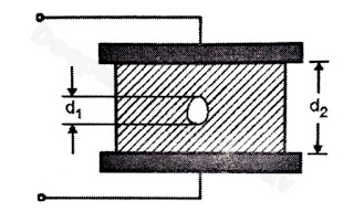
- Consider a dielectric material placed between two electrodes as shown in Figure A.
 |
| Figure A |
- When voltage is applied to the dielectric, the voltage stress appearing across the void is significantly higher than the remaining mass of the dielectric.
- This is because the dielectric constant of void is considerably less than surrounding dielectric.
- If the voltage across the void increases above corona inception voltage (CIV) of the gas present in the void, the partial discharge takes place across the void.
- This can cause progressive deterioration of the dielectric material. The equivalent circuit of this process is represented in Figure B.
 |
| Figure B |
- CV represents capacitance of void and CY represents capacitance of dielectric in series with void.
- Cb represents capacitance of remaining mass of dielectric.
- When partial discharge takes place, high frequency current are produced for a very short duration of time and after discharge, this current disappears.
- Let applied voltage across the dielectric is V volt and the voltage across void is V1 volt.
d1 = thickness of dielectric
d2 = thickness of dielectric
∈0 = permittivity of void air medium
∈r = permittivity of dielectric medium
∈1 = ∈0 ∈r
 |
| Figure C |
V1 = Vd1/d1+ (∈0/
∈1)d2

